Memory Packaging Market is estimated to be valued at USD 32.33 Bn in 2025 and is expected to reach USD 52.98 Bn in 2032, exhibiting a compound annual growth rate (CAGR) of 7.31% from 2025 to 2032. The memory packaging market is a rapidly growing on the account of increasing demand for memory chips in mobile devices and other applications such as telematics, data centers, automotive, and consumer electronics. The market also getting benefit from a number of technological advancements that are being made in the field of electronic circuitry.
Global Memory packaging Market: Regional Insights
Based on geography, the global memory packaging market is segmented into North America, Europe, Asia Pacific, Latin America, and Middle East & Africa.
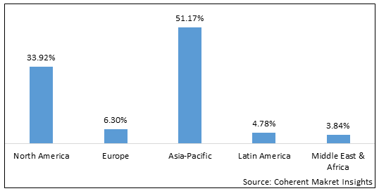
North America is expected to dominate the global memory packaging market over the forecast period owing to the strong growth of consumer electronics sector in the US. According to the consumer electronics association, the consumer electronics industry in the United States is estimated to grow by 3.9% in size from 2018 to 2019, reaching a total of US$ 398 billion in retail revenue
Asia Pacific is expected to witness fastest growth in the global market over the forecast period as it is home to some of the leading manufacturing hubs and thriving technology companies. The region also has a strong base of suppliers, foundries, and end users of advanced semiconductor packaging products. According to SEMI, China may top the rest of the world in fab investment, by 2020, with more than US$ 20 billion in spending, driven by memory and foundry projects, funded by both multinational and domestic companies. Currently, 25 new fab construction projects are planned in China. About 17 - 300 mm fabs are being tracked as part of this investment and expansion activity. This is anticipated to impact the memory packaging market’s growth positively, over the forecast period.
Figure 1. Global Memory packaging Market, By Region 2025

To learn more about this report, Download Free Sample
Global Memory packaging Market Drivers:
Growing demand for data center driven by cloud and HPC application to foster market growth
Increased adoption of DRAM in the data center is expected to positively impact the market growth. According to the Coherent Market Insights analysis, by 2020, it is anticipated that the major global data centers would begin more than ten construction projects worldwide, of which, more than 80% are expected to be initiated by the North America data center market, which is expected to boost the demand for server DRAM. Moreover, in response to the new data center construction projects carried out by Google, Amazon Web Service, Facebook, and Microsoft Azure, Intel and AMD have introduced new server processors in 2018. Hence, growing demand for date center is expected to drive market growth.
Rising demand for smartphone and changing technology is augmenting market growth
The memory packaging is gaining high adoption in manufacturing of smartphone due to recent advancement in silicon wafer that have enabled the process of wafer level packaging (WLP), where IC is packaged while it is a component of the wafer. For example, the case of Apple’s iPhones, the 2007 version of iPhone involved just two wafer level packaging. By the time of the third iteration of iPhones (iPhone 5), the device consisted of seven wafer level packages in the device.
Global Memory packaging Market Opportunities:
Growing popularity of TSV type memory packaging to present lucrative market opportunities. TSV is a highly efficient packaging method that uses a single layer of silicon to hold memory chips. This type of packaging is currently used in many memory chips, and it is expected to remain the dominant type for the foreseeable future. It is used in memory chips requiring high bandwidth and low latency for high performance computing applications.
Rise in manufacturing activities in China and India is expected to bring bright market opportunities for key players in memory packaging market. According to the India Brand Equity Foundation, India’s gross domestic product (GDP) at current prices stood at Rs. 51.23 lakh crore (US$ 694.93 billion) in the first quarter of FY22, as per the provisional estimates of gross domestic product for the first quarter of 2021-22. The manufacturing GVA at current prices was estimated at US$ 77.47 billion in the third quarter of FY22 and has contributed around 16.3% to the nominal GVA of during the past ten years.
Memory Packaging Market Report Coverage
| Report Coverage | Details | ||
|---|---|---|---|
| Base Year: | 2024 | Market Size in 2025: | USD 32.33 Bn |
| Historical Data for: | 2020 To 2024 | Forecast Period: | 2025 To 2032 |
| Forecast Period 2025 to 2032 CAGR: | 7.31% | 2032 Value Projection: | USD 52.98 Bn |
| Geographies covered: |
|
||
| Segments covered: |
|
||
| Companies covered: |
Tianshui Huatian Technology Co Ltd, Hana Micron Inc., lingsen precision industries Ltd, Formosa Advanced Technologies Co. Ltd (FATC), Advanced Semiconductor Engineering Inc. (ASE Inc.), Amkor Technology Inc., Jiangsu Changjiang Electronics Technology Co. Ltd, Powertech Technology, King Yuan Electronics Corp. Ltd, ChipMOS Technologies Inc., TongFu Microelectronics Co., and Signetics Corporation |
||
| Growth Drivers: |
|
||
| Restraints & Challenges: |
|
||
Uncover macros and micros vetted on 75+ parameters: Get instant access to report
Global Memory packaging Market Trends:
Miniaturization of semiconductor device is a recent trend
Miniaturization is a key trend in electronic device fabrication that is enabling new technological devices to be built, from portable computers and smartphone technology to smart medical devices. The key process of semiconductor miniaturization is called exposure, which involves using precision optical instrument to transfer a circuit pattern of elements and interconnections to a wafer.
Advent of artificial intelligence (AI)-based mobile applications and 5G technology
The launch of artificial intelligence (AI)-based mobile applications and 5G technology is projected to growth worldwide with a high volume of investments from the respective companies. As the above-mentioned technologies evolve, the need for power and energy reduction in mobile devices will drastically increase. This will create demand for exceptional DRAM which in turn augment the growth of the market.
Global Memory packaging Market Restraints:
Challenges landscape of the OSAT industry to restrict market growth
The memory packaging is associated with integrated device manufacturers (IDMs) and the outsourced semiconductor assembly and test company (OSATS). The trade tensions between the China and United States have already led to some packaging houses to slow their funds in China. This factor is expected to hinder the market growth. However, memory packaging market continues to gain momentum, especially with the approaches, such as 3D, 2.5D, fan-out and system-in-package (SIP).
Limited capacity and higher power consumption of memory packaging to hinder market growth
The disadvantages of memory packaging include limited capacity, higher power consumption, and increased thickness limit. Such limitations are expected to hamper the adoption of technology thereby hindering market growth.
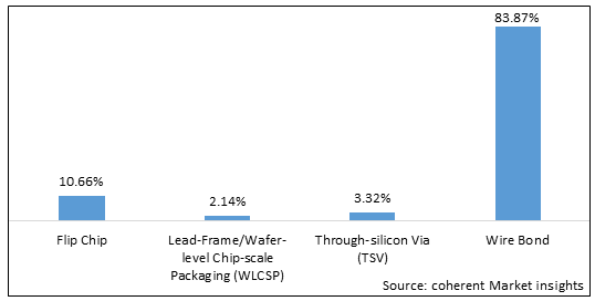
Figure 2. Global Memory packaging Market, By Platform 2025

To learn more about this report, Download Free Sample
Global Memory packaging Market Segmentation:
The global memory packaging market report is segmented into platform, application, end user, and region
Based on platform, the market is segmented into Flip-chip, Lead-frame, Wafer-level Chip-scale Packaging (WLCSP), Through-Silicon Via (TSV), and Wire-bond. Out of which, Flip-chip is expected to dominate the global market over the forecast period and this is attributed to its low power cost and high-density packaging. It has potential to replace traditional packaging technology.
Wafer-level Chip-scale Packaging segment is also expected to witness significant growth in the near future. WLSCP is the most commonly employed packaging for NOR flash and niche memory devices, such as EPROMs/EPROM/ROM. It is actively used in non-memory chips, such as application processors and power management integrated circuits (PMICs), to reduce the thickness of the package, which can improve heat dissipation.
Based on application, the market is segmented into NAND Flash Packaging, NOR Flash Packaging, DRAM Packaging, and Other Applications. Out of which, NAND Flash Packaging is expected to dominate the global market over the forecast period. Flash memory is a key component in mobile devices such as smartphones and tablets, with the average smartphone containing 43GB of NAND storage.
NOR Flash Packaging segment is also expected to witness significant growth in the near future. NOR flash is an embedded memory device that supports random-access read and write operations. This feature is a boon for complex embedded devices that rely on fast code execution
Based on end user, the market is segmented into IT and Telecom, Consumer Electronics, Embedded Systems, Automotive, and Other End Users. Out of which, IT and Telecom is expected to dominate the global market over the forecast period and this is attributed to the rapid adoption of 5G technology and innovation in wireless communication.
Consumer Electronics segment is also expected to witness significant growth in the near future owing to the increasing usage of smartphone, laptops, tablets, and other electronic devices. According to We are Social’s Digital in 2018, the unique mobile users was 5.135 billion.
Global Memory packaging Market: Key Developments
In October 2022, TSMC announced the Open Innovation Platform® (OIP) 3DFabric Alliance at the 2022 Open Innovation Platform Ecosystem Forum. The new TSMC 3DFabric™ Alliance is TSMC’s sixth OIP Alliance and the first of its kind in the semiconductor industry that joins forces with partners to accelerate 3D IC ecosystem innovation and readiness, with a full spectrum of best-in-class solutions and services for semiconductor design, memory modules, substrate technology, testing, manufacturing, and packaging.
Global Memory packaging Market: Key Companies Insights
The global memory packaging market is highly competitive. This is attributed to continuous launch of new technologies due to ongoing R &D and efforts by value chain participants. Moreover, key players are adopting various business growth strategies in order to expand their presence on regional as well as global basis. Some of the key players in the global memory packaging market are Tianshui Huatian Technology Co Ltd, Hana Micron Inc., lingsen precision industries Ltd, Formosa Advanced Technologies Co. Ltd (FATC), Advanced Semiconductor Engineering Inc. (ASE Inc.), Amkor Technology Inc., Jiangsu Changjiang Electronics Technology Co. Ltd, Powertech Technology, King Yuan Electronics Corp. Ltd, ChipMOS Technologies Inc., TongFu Microelectronics Co., and Signetics Corporation
*Definition: The memory packaging is a technology that is used to memory devices are packaged. There are wide range of packaging technologies available such as flip-chip, lead frame, wire-bond, through-silicon via (TSV) and wafer level chip-scale packaging (WLCSP).
Share
Share
About Author
Kalpesh Gharte is a senior consultant with approximately 5 years of experience in the consulting industry. Kalpesh holds an MBA in Operations and Marketing Management, providing him with a strong foundation in market strategy and analysis. He has contributed to various consulting and syndicated reports, delivering valuable insights that support informed business decisions
Missing comfort of reading report in your local language? Find your preferred language :
Transform your Strategy with Exclusive Trending Reports :
Frequently Asked Questions
Select a License Type
Joining thousands of companies around the world committed to making the Excellent Business Solutions.
View All Our Clients