Epitaxial Wafer Market is estimated to be valued at USD 3,997.8 Mn in 2025 and is expected to reach USD 9,347.1 Mn in 2032, exhibiting a compound annual growth rate (CAGR) of 12.9% from 2025 to 2032. Epitaxial Wafer, otherwise called Epi-wafer is put over other silicon wafer through epitaxial process. Epitaxy is the process of depositing a monocrystalline silicon layer over a silicon wafer's polished crystal surface. On top of a polished wafer, layers of single silicon carbide crystals many micrometers thick are added to make an epitaxial wafer. Its seamless production necessitates precise control over thickness, carrier concentration, and defect density.
Compound semiconductor epitaxial wafers are processed to produce chips and integrated circuits (ICs), which can be found in a wide range of technological gadgets worldwide. The wireless, photonic, and electronic performance of the wafers is determined by the epitaxial layers.
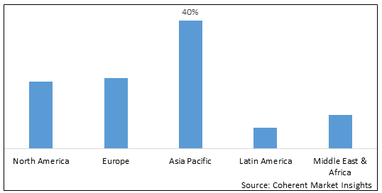
Figure 1: Epitaxial Wafer Market Share (%), By Region 2025

To learn more about this report, Download Free Sample
Epitaxial Wafer Market: Regional Insights
In 2025, the epitaxial wafer market in Asia-Pacific held the largest share of the global market. This market's expansion can be attributed to a variety of factors, including the growing use of IoT, self-driving cars, and smartphone penetration. Thicker and smaller integrated circuits (ICs) have emerged as a result of rising smartphone demand and advancements in smartphone technology. The building blocks of semiconductors are these silicon wafers, and semiconductor devices or chips are made on these substrates. Computers, consumer electronics, telecommunications products, and other electronic devices all make use of these semiconductors. As a result, manufacturers are coating this wafer with epitaxial wafer to boost the power of these electronic devices in response to rising demand. As a result, it is anticipated that this factor will increase demand for epitaxial wafer in the region over the anticipated time frame.
In addition, this region is the largest consumer of semiconductor integrated circuits due to the presence of significant manufacturers like Samsung, Sony, LG, Toshiba, Panasonic, Toyota, and Honda. IC production is accelerated when players are present. As a result, there will be an increase in demand for epitaxial wafer in this particular region as a result of this.
Epitaxial Wafer Market Drivers:
Increase in Adoption of LED lighting
The rising demand for epitaxial wafer is being fueled by the widespread adoption of LED lighting, which is a major driver of market expansion. LED light bulbs are more long-lasting, durable, and comparable to or superior to other types of lighting. In contrast to incandescent and compact fluorescent lights (CFLs), which produce heat and light in all directions, LEDs are "directional" light sources. As a result, LEDs can utilize light and energy more effectively in numerous applications. They produce less heat and consume less energy than incandescent bulbs. A few LEDs can work at generally 10% of the power expected for the standard light and last up to quite a bit longer.
Epitaxial Wafer Market Report Coverage
| Report Coverage | Details | ||
|---|---|---|---|
| Base Year: | 2024 | Market Size in 2025: | USD 3,997.8 Mn |
| Historical Data for: | 2020 To 2024 | Forecast Period: | 2025 To 2032 |
| Forecast Period 2025 to 2032 CAGR: | 12.9% | 2032 Value Projection: | USD 9,347.1 Mn |
| Geographies covered: |
|
||
| Segments covered: |
|
||
| Companies covered: |
EpiWorks Inc., Global Wafers Japan Co. Ltd., Nichia Corporation, SHOWA DENKO K.K., Siltronic AG, Desert Silicon Inc., Electronics and Materials Corporation Ltd. Intelligent Epitaxy Technology Inc.IQE plc., Jenoptic AG, MOSPEC Semiconductor Corporation, Norstel AB, Ommic S.A., Silicon Valley Microelectronics Inc., SVT Associates Inc. Universal Wafer Inc., Wafer Works Corporation, Xiamen Powerway Advanced Materials Co. Ltd., and Visual Photonics Epitaxy Co. Ltd |
||
| Growth Drivers: |
|
||
| Restraints & Challenges: |
|
||
Uncover macros and micros vetted on 75+ parameters: Get instant access to report
Initial high capital investments
The term "initial capital investment" refers to the cost of purchasing or building a power or non-power facility that is expected to be repaid from power revenues. This includes, but is not limited to, any costs associated with planning, designing, purchasing land, and building, investing during construction, and testing. Initial high capital investments will restrict small players to enter in the semiconductor manufacturing sector. This factor will further restrict growth of epitaxial wafer market in the near future.
Epitaxial Wafer Market Restraints:
Higher cost of wafer fabrication
In the semiconductor device fabrication process, wafer fabrication is a process that consists of numerous repeated, sequential processes to produce complete electrical or photonic circuits on semiconductor wafers. The disservices of epitaxy incorporate greater expense of wafer manufacture, extra cycle intricacies, and issues related with surrenders in the epi layer. A semiconductor processing facility that converts wafers into integrated circuits is known as a wafer fab. Conductors, transistors, resistors, and other electronic components on a semiconductor wafer are defined by a complex series of steps in a typical wafer fab.
Segment graph
Figure 2: Epitaxial Wafer Market Share (%), By Application, 2025

To learn more about this report, Download Free Sample
Epitaxial Wafer Market Segmentation:
The global Epitaxial Wafer Market report is segmented into By Deposition Type, By Wafer Size and By Application
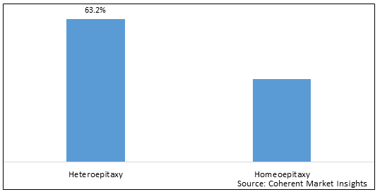
Based on By Deposition Type, the market is segmented Heteroepitaxy, and Homeoepitaxy, Based on Wafer Size, the market is segmented into 50mm to 100mm, 100mm to 150mm, above 150mm, Based on Application, and the market is segmented into LED Semiconductor, Power Semiconductor, MEMS-based devices.
Epitaxial Wafer Market: Key Companies Insights
Imec and Qromis have teamed up for the created improvement mode, p-GaN discrete, and IC power gadgets on 200 mm QST substrates, with epitaxy layers filled in Aixtron's G5+ C 200 mm MOVCD stage. In an advanced CMOS silicon pilot line, both businesses have been working on device fabrication, developing GaN power devices, discrete and monolithically integrated IC forms, and 200 mm QST substrates. Imec and Qromis have teamed up with Germany-based GaN MOCVD gear maker, Aixtron on GaN-on-QST epitaxy advancement. According to a number of industry experts, the number of integrated circuit (IC) semiconductor fabrication plants that process 300 mm wafers will increase from 15 in 2002 to 138 in 2023.
Epitaxial Wafer Market Key Developments:
May 2020 - SweGaN AB, a company that produces custom gallium nitride on silicon carbide (GaN-on-SiC) epitaxial wafers for RF and power electronics devices, has announced a new benchmark for GaN high-frequency devices based on its QuanFINE material. The company believes that the demonstration promises commercial benefits for the entire GaN RF value chains, which include telecom, space, and military markets.
Global Wafers Taiwan CO in June 2022 Ltd has announced a $5 billion investment in a Texas plant that will produce and supply locally produced 300-millimeter silicon wafers for semiconductors.
*Definition: For use in photonics, microelectronics, spintronics, or photovoltaics, an epitaxial wafer, also known as an epi-wafer, epi-wafer, or epiwafer, is a wafer of semiconducting material created through epitaxial growth (epitaxy).Epi wafers are used for component of diode and semiconductor or substrate for IC, for example, bipolar sort and MOS type. In addition, power devices frequently make use of multiple layer epi wafers and thick film epi wafers, both of which contribute to the compactness and energy efficiency of various power source products.
Share
Share
About Author
As an accomplished Senior Consultant with 7+ years of experience, Pooja Tayade has a proven track record in devising and implementing data and strategy consulting across various industries. She specializes in market research, competitive analysis, primary insights, and market estimation. She excels in strategic advisory, delivering data-driven insights to help clients navigate market complexities, optimize entry strategies, and achieve sustainable growth.
Missing comfort of reading report in your local language? Find your preferred language :
Transform your Strategy with Exclusive Trending Reports :
Frequently Asked Questions
Select a License Type
Joining thousands of companies around the world committed to making the Excellent Business Solutions.
View All Our Clients