Chemical Vapor Deposition Market Analysis & Forecast: 2025-2032
Global Chemical Vapor Deposition Market size is estimated to be valued at USD 26.53 Bn in 2025 and is expected to reach USD 49.47 Bn by 2032, exhibiting a compound annual growth rate (CAGR) of 9.3% from 2025 to 2032.

To learn more about this report, Download Free Sample
Key Takeaways
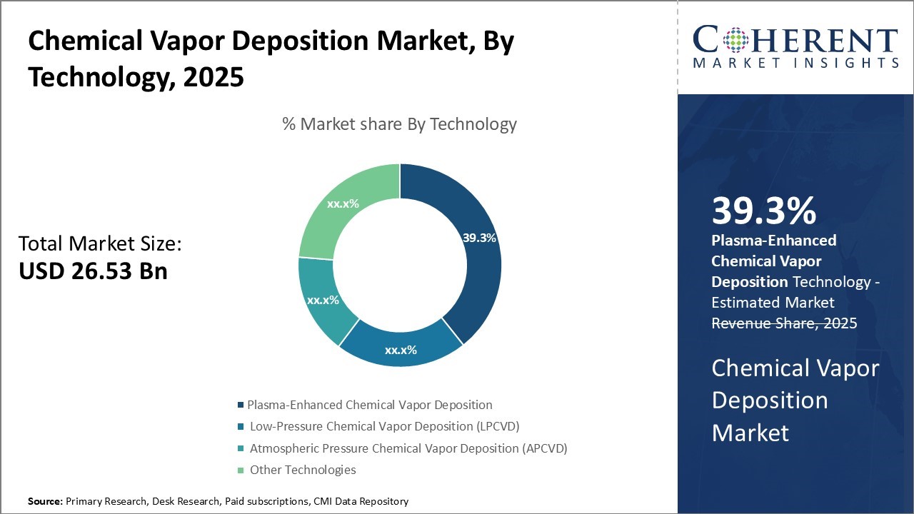
- By Technology, The PECVD segment is expected to lead the share in the chemical vapor deposition market with a 39.3 % share in 2025. This growth is driven by PECVD’s specific advantages such as improved film quality and processing at lower temperatures relative to other deposition methods.
- By Application, the semiconductors segment is expected to dominate the share of 38.2% in 2025, as chemicals vapor deposition remains an important process in the manufacture and advanced chip the semiconductor device.
- By Region, North America stands to gain significant Chemical Vapor Deposition Market share to the tune of 40.9% in 2025 due to its established high-technology semiconductor fabrication facilities and widespread adoption of newer technologies
Market Overview
Global Chemical Vapor Deposition Market growth is driven by growing demand for chemical vapor deposition equipment across various industries like electronics, machinery, and medical devices. Technological advancements are enabling higher process through put and uniform nano coatings at nano-scale levels. Key players such as Applied Materials, Inc., Lam Research Corporation and other are investing in Research and Development R&D to develop new deposition materials and reduce cost of ownership.
Current Events and Its Impact
|
Event |
Description and Impact |
|
Geopolitical Tensions and Trade Policies |
|
|
Regulatory and Supply Chain Shifts |
|
|
Technological Innovations |
|
Uncover macros and micros vetted on 75+ parameters: Get instant access to report
Emerging Innovations in Chemical Vapor Deposition Market
Chemical Vapor Deposition (CVD) technologies are increasingly expanding into specialized applications with significant untapped potential. These emerging niches offer manufacturers and market participant’s valuable opportunities for differentiation and sustainable growth.
Emerging Applications
- Biocompatible Medical Implant Coatings: The use of CVD for depositing titanium nitride and diamond-like carbon coatings on dental and orthopedic implants is increasing. These coatings augment wear resistance and Osseo integration, serving to enhance the performance as well as the longevity of the implant. Even though adoption is limited to specialized implant manufacturers, solutions have been commercialized by companies like IBC Coatings Technologies.
- Low-Temperature Epitaxial Growth (LEPECVD): With LEPECVD, it is possible to deposit epitaxial semiconductor layers of high quality onto substrates with temperatures below 800°C. This is crucial for processing heat-sensitive substrates used in MEMS devices and advanced photonics. Research institutions like Fraunhofer IISB actively employ this technique, but it is only beginning to gain traction among industrial users.
- Aerospace Component Protection: The use of CVD deposited alumina and silicon carbide coatings for enhanced oxidation resistance on turbine blades in hypersonic aircraft is under evaluation. These coatings are being tested by major industry players such as Rolls-Royce and GE Aviation, but other aerospace component protection, which is dominated by thermal spray methods, still uses traditional techniques.
Future Applications
- Solid-State Battery Electrolytes: The application of CVD techniques for Li Lanthanum Zirconium Oxide (LLZO) thin films is intended to avoid macroscopic dendrite growth in solid state batteries. Patents on related processes have also been filed by firms such as BMW and QuantumScape.
- Quantum Computing Components: The development of CVD tools for deposition of superconducting niobium-tin films that are necessary for the development of qubits for quantum computers has been pioneered by Aixtron and Oxford Instruments.
- Self-Healing Tribological Coatings: CVD MXene coatings capable of self-repair of microcracks under severe conditions can change the durability of machinery across industries, according to MIT Lincoln Laboratory Research.
Advanced CVD Market, integrating sustainable and high-tech, helps industry players to set higher prices claiming first-mover advantages. These markets with emerging technologies, coupled with robust collaboration between end-users and equipment manufacturers, present significant value potential.
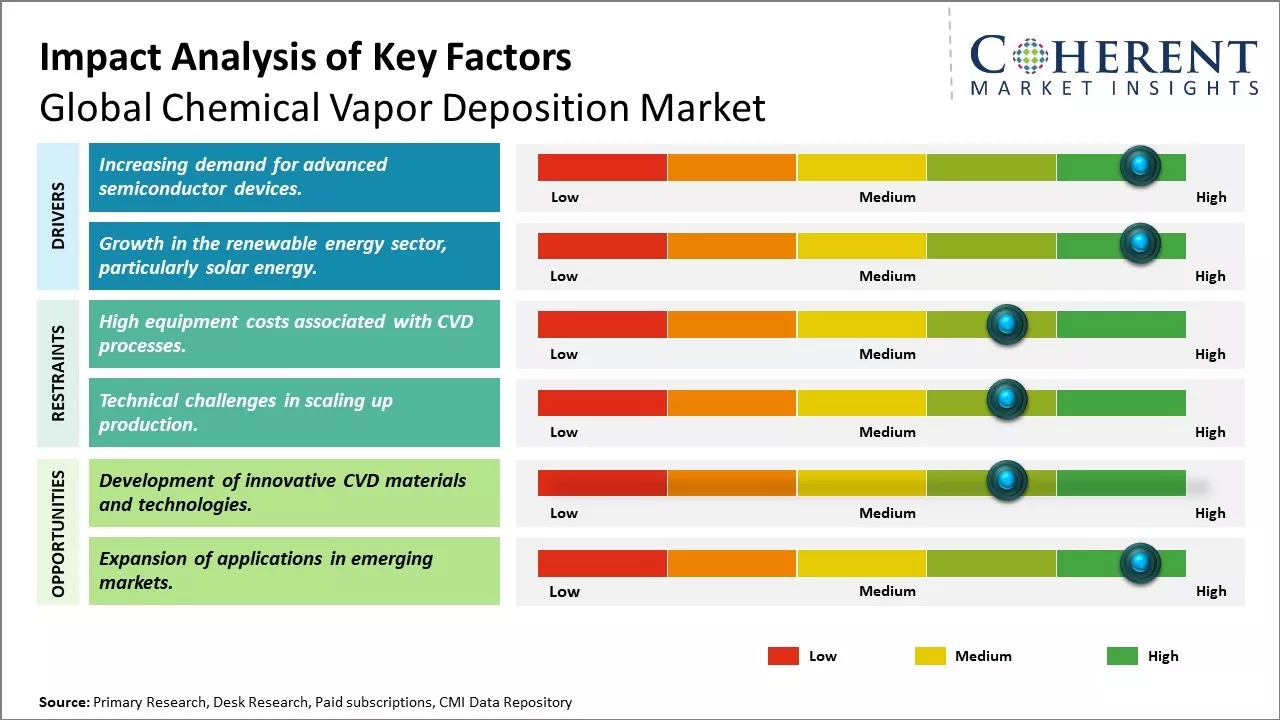
Increasing demand for advanced semiconductor devices
The ubiquitous presence of electronic devices in our lives has meant that the demand for more advanced and powerful semiconductor chips is ever increasing. In applications ranging from smartphones to artificial intelligence, there is a constant push for higher performance and lower power consumption from semiconductors.
One of the major ways to deposit materials in semiconductor manufacturing is Chemical Vapor Deposition (CVD). It enables the uniform deposition of thin films on wafers through a chemical reaction between vapor phase substances and the surface of the substrate. Developments such as Plasma Enhanced Chemical Vapor Deposition (PECVD) have made it possible to exert angstrom-level control over film thickness at remarkable speeds. As the number of functions integrated into chips increases with each generation, conventional methods of deposition are struggling to keep up with the demands. This is accelerating the adoption of atomic layer deposition (ALD) – a type of CVD that is capable of depositing thin, precise monolayers of materials.
In addition, the need for 3D architectures like high aspect ratio structures requires seamless, conformal, thin film coverage which is difficult for CVD to accomplish. Newer generation technologies for deposition such as spatial ALD are designed to improve this by allowing individual dosing of precursor gases to specific locations on the substrate.
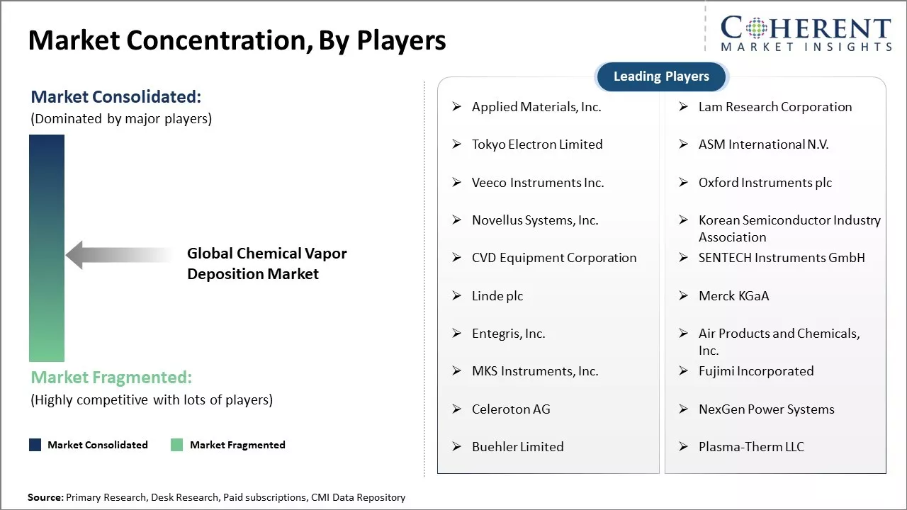
Market Concentration and Competitive Landscape

To learn more about this report, Download Free Sample
Growth in the Renewable Energy Sector, Particularly Solar Energy
Across the globe, there is an increasing propensity to develop sustainable energy sources in order to replace fossil fuels and mitigate the carbon footprint. Renewable energy is at the forefront of the transition as solar energy has the fastest increasing rate of new installations and subsidizing costs.
For example, data from the International Energy Agency indicates that the supply of renewable energy (solar, wind, hydro, geothermal and ocean) increased by almost 8% in 2022. This resulted in an increase in the share of renewable energy in the total global energy supply which increased by about 0.4 percentage points reaching 5.5% is on the rise. It is notable that this trend signifies the increasing importance of renewable resources in the global energy market and indicates the shift towards more environmentally friendly sources of energy.
Chemical vapor deposition (CVD) is an essential step in the production of crystalline silicon solar cells. It pertains to the formation of films of silicon, silicides and oxides that constitute the core p-n junctions and passivation layers on silicon wafers. If the goal of the solar sector is higher efficiency conversion rates exceeding 25%, precision with lower bounds CVD films and interfaces is critical. However, these systems must meet manufacturability with high deposition rates and reproducibility.
Market Opportunity
- Development of innovative CVD materials and technologies
The development of innovative new materials and continuous advancement in CVD technologies present significant opportunities for future Chemical Vapor Deposition Market Growth. CVD allows for customization of material properties at the nano-scale and deposition of multi-layer thin films.
Extensive R&D is ongoing to expand the portfolio of CVD materials beyond the mainstream silicon, ceramics and metals. Novel materials such as graphene and 2D chalcogenides deposited using CVD show promise for a wide range of applications. Advancement in precursors and precursor delivery technologies improve film deposition control at the atomic level. Furthermore, new reactor designs with improved thermal budget and compatibility with large-area or 3D substrates expand the CVD application scope.
Continued innovation in CVD processes, such as remote or spatial ALD, open up new avenues for cost reductions. The emerging applications of CVD films in advanced electronics, renewable energy, protective coatings and biomaterials point towards substantial future demands. This provides ample opportunities for CVD vendors to strengthen their market position.
Chemical Vapor Deposition Market Insights, by Technology
In terms of technology, the plasma-enhanced chemical vapor deposition (PECVD) segment is estimated to contribute the highest Chemical Vapor Deposition Market Demand share in 2025, owing to its unique advantages over competing deposition techniques. PECVD allows for more precise control of film thickness and uniformity during the deposition process.
Unique capabilities for depositing films at lower temperatures are especially valuable for applications involving heat-sensitive materials. The ability to create conformal coatings on complex three-dimensional substrates makes PECVD well-suited for integrated circuit manufacturing where film deposition must occur in high-aspect ratio trenches and holes.
Chemical Vapor Deposition Market Insights, by Application
In terms of application, the semiconductors segment is estimated to contribute the highest Chemical Vapor Deposition Market Outlook share of 38.2% in 2025, due to the central role of chemical vapor deposition in the semiconductor manufacturing industry. CVD is used for depositing numerous functional thin films during the fabrication of integrated circuits, memory chips, and other devices.
Some of the most common CVD applications in semiconductor processing include depositing conducting films like tungsten, aluminum, and copper used for transistors, wires, and other conductive elements. CVD also excels at dielectric films deposition, with silicon oxide and nitride being workhorse materials for insulation and passivation layers. Meanwhile, developing new electric device architectures requires CVD to deposit novel materials like high-k dielectrics for advanced CMOS gate oxides.
Regional Insights

To learn more about this report, Download Free Sample
North America Chemical Vapor Deposition Market Analysis and Trends
North America is poised to dominate the global Chemical Vapor Deposition Market Value, projected to account for 40.9% of the global share in 2025. This regional leadership is primarily attributed to a strong presence of leading semiconductor manufacturers such as Intel, Qualcomm, and Micron, which maintain robust manufacturing operations within the U.S. to cater to growing local demand across electronics, automotive, and industrial applications.
Asia Pacific Chemical Vapor Deposition Market Analysis and Trends
The growth of the Chemical Vapor Deposition Market Forecast will be remarkable in the Asia Pacific region when forecasted. There is a large scale adoption of CVD technologies across the region because China, Japan, South Korea and Taiwan have turned into prominent hubs for semiconductor and electronic manufacturing.
China’s policies like “Made in China 2025” strengthen their technology supply chains by self-sufficiently fabricating local technology. These policies are supporting domestic fabrication. India is also emerging with high potential due to rapid growth in the electronics and automotive sectors. With 28.43 million vehicles produced in FY 2023–2025, India became the world’s third largest automobile market by sales, according to Invest India.
Dominating Countries in the Chemical Vapor Deposition Market
United States Chemical Vapor Deposition Market Analysis and Trends
The U.S. remains the central force behind North America's leadership in the Chemical Vapor Deposition Market Trends. With established semiconductor giants and a strong presence of CVD equipment manufacturers, the country continues to see robust demand for thin-film technologies across chipmaking, solar energy, and industrial applications. Continuous advancements in manufacturing nodes and sustained capital investments keep the U.S. at the forefront of CVD innovation and deployment.
India Chemical Vapor Deposition Market Analysis and Trends
India is gaining traction as a rising market in the Asia Pacific region. The country’s growing electronics and automotive production is generating increased demand for high-performance coating and deposition technologies. Supportive policies and infrastructure development are encouraging global semiconductor and component manufacturers to expand operations in India, thereby enhancing the country’s contribution to the regional and global CVD market.
Market Report Scope
Chemical Vapor Deposition Market Report Coverage
| Report Coverage | Details | ||
|---|---|---|---|
| Base Year: | 2024 | Market Size in 2025: | USD 26.53 Bn |
| Historical Data for: | 2020 To 2024 | Forecast Period: | 2025 To 2032 |
| Forecast Period 2025 to 2032 CAGR: | 9.3% | 2032 Value Projection: | USD 49.47 Bn |
| Geographies covered: |
|
||
| Segments covered: |
|
||
| Companies covered: |
Applied Materials, Inc., Lam Research Corporation, Tokyo Electron Limited, ASM International N.V., Veeco Instruments Inc., Oxford Instruments plc, Novellus Systems, Inc., Korean Semiconductor Industry Association, CVD Equipment Corporation, SENTECH Instruments GmbH, Linde plc, Merck KGaA, Entegris, Inc., Air Products and Chemicals, Inc., MKS Instruments, Inc., Fujimi Incorporated, Celeroton AG, NexGen Power Systems, Buehler Limited, and Plasma-Therm LLC |
||
| Growth Drivers: |
|
||
| Restraints & Challenges: |
|
||
Uncover macros and micros vetted on 75+ parameters: Get instant access to report
Analyst viewpoints
- Global chemical vapor deposition market is poised to grow substantially over the next decade driven by the rising demand for integrated circuits from the semiconductor and electronics industries. CVD is increasingly becoming the preferred deposition technique over other methods due to its ability to provide high-quality and precise thin film coatings. The development of new advanced materials like graphene which requires highly uniform thin films will further propel the demand for CVD.
- However, stringent environmental regulations around hazardous gases like dichlorosilane used in the CVD process can restrain the market growth. High initial investment and maintenance costs of CVD equipment also remains a major challenge. Nonetheless, emerging technologies like 3D printing and 5G networks will open up new revenue streams for CVD manufacturers.
- The North America region, currently dominates the global CVD market owing to presence of large fabs and outsourced foundries while Asia Pacific is fasting growing region in the market. Moving forward, North America is expected attract significant investments as companies try to shorten supply chains and onshore more production.
Chemical Vapor Deposition Industry News
- In November 2024, CVD Equipment Corporation received a follow-on order worth approximately $3.5 million for a production Chemical Vapor Infiltration (CVI) system, aimed at manufacturing advanced, energy-efficient materials for gas turbine engines.
- In 2023, AIXTRON announced an investment of approximately 100 million euros (USD 109.7 million) at its Herzogenrath site. This substantial investment is aimed at constructing an innovation center designed to significantly enhance the company's research and development capabilities. The new facility is expected to focus on deposition equipment manufacturing for the semiconductor industry, providing key players in the semiconductor market with expanded capacities for innovation and development. By establishing this center, AIXTRON reinforces its commitment to advancing technology and supporting the growth of the semiconductor sector, positioning itself as a leader in this critical industry.
Market Segmentation
- By Technology Insights (Revenue, USD Bn, 2020 - 2032)
- Plasma-Enhanced Chemical Vapor Deposition (PECVD)
- Low-Pressure Chemical Vapor Deposition (LPCVD)
- Atmospheric Pressure Chemical Vapor Deposition (APCVD)
- Other Technologies
- By Application Insights (Revenue, USD Bn, 2020 - 2032)
- Semiconductors
- Solar Cells
- Optical Coatings
- Medical Devices
- Others
- Regional Insights (Revenue, USD Bn, 2020 - 2032)
- North America
- U.S.
- Canada
- Latin America
- Brazil
- Argentina
- Mexico
- Rest of Latin America
- Europe
- Germany
- U.K.
- Spain
- France
- Italy
- Russia
- Rest of Europe
- Asia Pacific
- China
- India
- Japan
- Australia
- South Korea
- ASEAN
- Rest of Asia Pacific
- Middle East
- GCC Countries
- Israel
- Rest of Middle East
- Africa
- South Africa
- North Africa
- Central Africa
- North America
- Key Players Insights
- Applied Materials, Inc.
- Lam Research Corporation
- Tokyo Electron Limited
- ASM International N.V.
- Veeco Instruments Inc.
- Oxford Instruments plc
- Novellus Systems, Inc.
- Korean Semiconductor Industry Association
- CVD Equipment Corporation
- SENTECH Instruments GmbH
- Linde plc
- Merck KGaA
- Entegris, Inc.
- Air Products and Chemicals, Inc.
- MKS Instruments, Inc.
- Fujimi Incorporated
- Celeroton AG
- NexGen Power Systems
- Buehler Limited
- Plasma-Therm LLC
Sources
Primary Research Interviews
- Semiconductor equipment manufacturers (e.g., Applied Materials, Lam Research Corporation) [5]
- CVD technology providers specializing in advanced coatings
- Leading semiconductor foundries and IDMs
- Solar panel manufacturers leveraging CVD processes [5]
- Others
Databases
- SEMI (Semiconductor Equipment and Materials International) Industry Reports
- Others
Magazines
- Semiconductor Today (CVD process innovations)
- Advanced Materials & Processes (ASM International)
- Photonics Media (CVD applications in optics)
- Others
Journals
- Journal of Vacuum Science & Technology (AIP Publishing)
- Thin Solid Films (Elsevier)
- ACS Applied Materials & Interfaces
- Others
Newspapers
- Financial Times (semiconductor industry trends)
- The Wall Street Journal (advanced manufacturing insights)
- Nikkei Asia (APAC CVD market developments)
- Others
Associations
- SEMI (Semiconductor Equipment and Materials International)
- ASM International (materials engineering focus)
- Materials Research Society (MRS)
- International Solar Energy Society (ISES)
- Others
Public Domain Sources
- U.S. Patent and Trademark Office (USPTO) CVD-related patents
- U.S. Department of Energy (DOE) reports on thin-film technologies
- European Union Public Database for Advanced Materials
- National Institute of Standards and Technology (NIST) CVD guidelines
- Others
Proprietary Elements
- CMI Data Analytics Tool
- Proprietary CMI Existing Repository of Information (Last 8 Years)
*Definition: The global chemical vapor deposition market refers to the market for chemical vapor deposition (CVD) technology and services across the world. CVD involves depositing thin films or layers of material onto substrates using chemical reactions that occur on the surface of the substrates. It finds applications in the electronics, data storage, optics, solar energy, and optoelectronics industries for manufacturing semiconductors, silicon wafers, and other devices and components.
Share
Share
About Author
Vidyesh Swar is a seasoned Consultant with a diverse background in market research and business consulting. With over 6 years of experience, Vidyesh has established a strong reputation for his proficiency in market estimations, supplier landscape analysis, and market share assessments for tailored research solution. Using his deep industry knowledge and analytical skills, he provides valuable insights and strategic recommendations, enabling clients to make informed decisions and navigate complex business landscapes.
Missing comfort of reading report in your local language? Find your preferred language :
Transform your Strategy with Exclusive Trending Reports :
Frequently Asked Questions
EXISTING CLIENTELE
Joining thousands of companies around the world committed to making the Excellent Business Solutions.
View All Our Clients

