Atomic Force Microscope Market Size and Trends
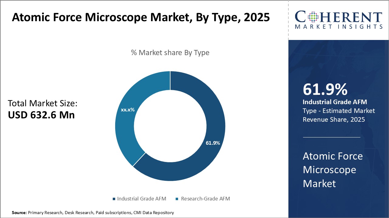
The atomic force microscope Market is estimated to be valued at USD 632.6 Mn in 2025 and is expected to reach USD 890.7 Mn by 2032, growing at a compound annual growth rate (CAGR) of 5.0% from 2025 to 2032.
Discover market dynamics shaping the industry: Download Free Sample
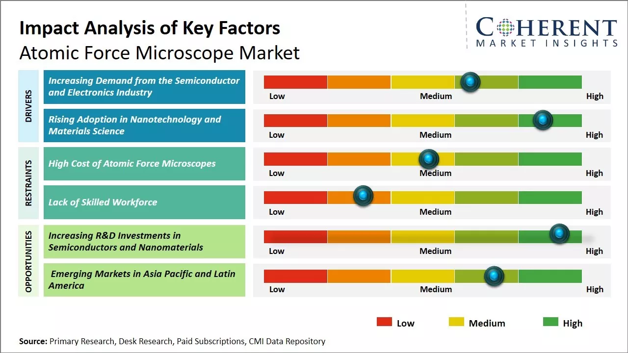
The atomic force microscope market is expected to witness a positive growth trend over the forecast period. The growing semiconductor and electronics industry and increasing use of atomic force microscope in the healthcare sector are expected to drive the market. Further, rising focus on developing high-resolution microscopes for applications, such as pathogen detection, protein mapping, and cell biology, is expected to support the growth of the atomic force microscope market during the forecast period. However, high cost of atomic force microscopes is a major factor that can hamper the growth of the market during the analysis period.
Increasing Demand from the Semiconductor and Electronics Industry
The increasing demand from the semiconductor and electronics industry is expected to be a key driver bolstering the growth of the atomic force microscope market over the forecast period. Atomic force microscopes have emerged as a critical tool to gain nanoscale insights into various materials and surfaces used in the manufacturing of semiconductors and electronic components. These microscopes allow manufacturers to examine and analyze microscopic defects as well as measure the thickness and surface roughness of thin film materials at an unprecedented resolution.
Given the ever-increasing miniaturization and integration of electronic components, manufacturers are under constant pressure to improve production processes, detect flaws, and ensure quality control at the nanolevel. Atomic force microscopes provide precise characterization of next-gen materials such as graphene and 2D materials that are revolutionizing the semiconductor industry. Various players in the industry extensively employ AFM to evaluate new material properties, gain quality control over manufacturing, and enable the development of more powerful and energy-efficient electronic devices. Furthermore, continual advances in consumer electronics and proliferation of IoT devices have also augmented the demand for more powerful yet smaller and efficient chips. This has significantly propelled the usage of atomic force microscopy in R&D as well as production facilities of chipmakers and electronics manufacturers.
For instance, Hitachi High-Tech Corporation, a nano-technology solutions provider, offers AFM5300E that meets the needs of the semiconductor industry by enabling AFM measurement in vacuum environments, along with high-resolution electromagnetism measurements and observation of dopant distribution.
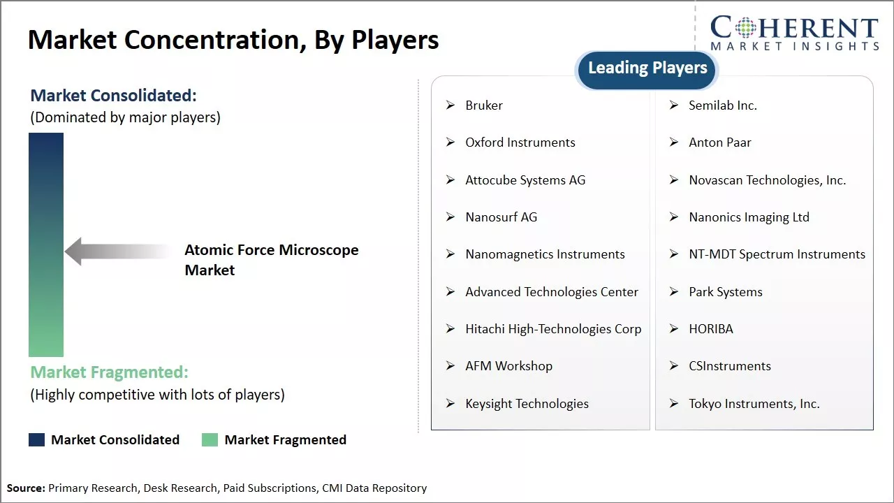
Market Concentration and Competitive Landscape
Get actionable strategies to beat competition: Download Free Sample
RisingAdoption in Nanotechnology and Materials ScienceThe rising adoption of atomic force microscopy in the field of nanotechnology and materials science is another key factor propelling the growth of the atomic force microscope market. Over the past few years, nanotechnology has emerged as one of the most important new general purpose technologies with widespread applications across various end-use industries including healthcare, energy, manufacturing, and consumer goods. Whether it is developing new materials with tailorable optical, electrical or mechanical properties or creating devices & systems with new functionalities, nanotechnology relies heavily on atomic force microscopy for characterization and analysis at the atomic scale.
AFM provides unmatched resolutions to visualize structures as small as individual atoms, gather topographic information on nano surfaces, and even manipulate matter at the nanoscale. It has, therefore, become indispensable for research associated with carbon nanotubes, nanoparticles, DNA sequencing as well as developing novel biomedical devices. AFM also finds extensive usage in various nanofabrication processes to control feature sizes, etch depths and uniformity during etching and lithography steps.
For instance, Oxford Instruments Asylum Research offers Cypher VRS1250 video-rate atomic force microscope (AFM). Its higher speed will enable researchers to capture nanoscale details of dynamic events that were previously inaccessible, including biochemical reactions, 2D molecular self-assembly, and etch and dissolution processes and more.
To learn more about this report, Download Free Sample
Market Challenges: High Cost of Atomic Force MicroscopesOne of the key challenges for the atomic force microscope market is the high cost of purchasing atomic force microscopes. As AFM systems are highly complex and use advanced nanoscale technologies, their pricing can be prohibitive for many small laboratories and research institutions. Additionally, operating and maintaining AFMs requires specialist knowledge and trained personnel. This increases utilization costs. Further, opportunities in certain application areas remain untapped as AFMs cannot image or characterize samples under liquid or gaseous environments.
Market Opportunities: Increasing R&D Investments in Semiconductors and Nanomaterials
The rising demand for nanotechnology and increasing R&D investments into applications like semiconductors, nanomaterials, and energy storage are driving more adoption of AFMs. Furthermore, the ability of AFMs to acquire 3D topographical information down to the atomic level with minimal sample preparation has led to many new users from industries like material science.
Discover high revenue pocket segments and roadmap to it: Download Free Sample
Insights, by Type - Industrial grade AFMs dominate the market due to their widespread use for quality control and assurance applicationsIndustrial grade AFM is estimated to contribute the highest share of 61.9% in 2025 in the market owing to the rising demand from manufacturing industries. Industrial grade atomic force microscopes are designed to handle routine industrial metrology tasks in manufacturing environments. They offer high stability, repeatability, and accuracy required to characterize surfaces, measure thickness, and evaluate production processes. The growing need for nanoscale characterization across diverse industrial settings such as semiconductor manufacturing, data storage media fabrication, and renewable energy equipment production is a key driver for the segment's growth.
Industrial grade AFMs are suitable for conducting high volume measurements as they feature ergonomic designs and easy to use software interfaces for non-specialist operators. Moreover, their robust and durable construction allows withstanding vibration and temperature variations common in production facilities. Leading manufacturers are also offering advanced in-situ imaging capabilities integrated with industrial AFMs to allow real-time inspection on the line without stopping production.
The rising complexities in nano-scale manufacturing bring more opportunities for adopting industrial AFMs. Their ability to conduct high resolution quality control at the earliest stages helps enhance yields and reduce costly reworks further down the assembly line. This improves process optimization and quality assurance. With nanotechnology finding increasing applications, the demand for metrology equipment capable of characterizing surfaces at nanoscale in industrial environments is expected to drive the industrial grade AFM segment.
For instance, Anton Paar GmbH, a manufacturer of laboratory instruments and process measuring systems, offers the atomic force microscope ToscaTM 400. This high-end product measures nano-surface properties and was specially designed for industrial users.
Insights, by Application - Semiconductors and electronics segment has been one of the major application areas for atomic force microscopes
Semiconductors and electronics is estimated to contribute the highest share of 34.7% in 2025 in the market owing to critical role in device development and fabrication. The semiconductors and electronics segment has been one of the major application areas for atomic force microscopes. The ability to non-destructively image surfaces at atomic or molecular resolution makes AFMs vital for the ongoing device scaling in semiconductor manufacturing.
During research and development, AFMs help characterize new materials and gain insights into surface properties at the smallest dimensions. This aids in engineering devices with tighter integration densities. Additionally, their application extends to failure analysis where AFM plays an important role in root cause identification of defects.
AFMs also find widespread usage in chip fabrication areas including lithography mask inspection, process monitoring, and quality control. Being a contactless technique, they do not damage fragile surfaces and are capable of characterizing even temporary structures key to fabricating next-generation devices.
The vast miniaturization occurring in electronics is propelling more extensive usage of AFMs across the whole fabrication line from developing novel materials to wafer inspection. Semiconductor foundries and integrated device manufacturers rely on AFMs to overcome technical challenges and reduce defects as critical dimensions shrink with each new technology node. This makes semiconductors and electronics a major driving application for the atomic force microscope market.
Regional Insights
Need a Different Region or Segment? Download Free Sample
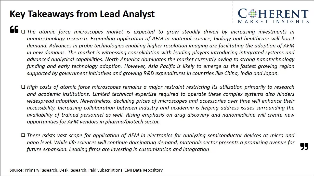
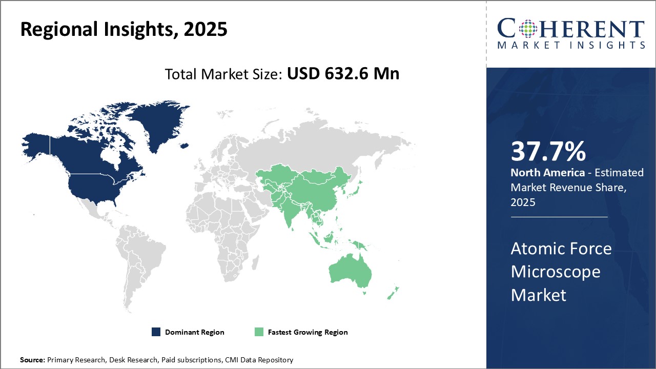
North America has established itself as the dominant regional market for atomic force microscopes globally. The region is estimated to hold the market share of 37.7% in 2025. The presence of major established players such as Bruker, Park Systems, and WITec has created a large installed base of AFMs in the region over the years. Strong funding for nanotechnology research from bodies like the National Science Foundation has driven significant demand from the life sciences and material science sectors.
Universities and national labs across the U.S. and Canada actively utilize AFMs for applications such as virus detection, material property measurement, and semiconductor analysis. Several upgrades and expansions to existing AFMs have also been undertaken to study newer areas like 2D materials and semiconductor device structures. The availability of skilled workforce and strong research infrastructure have ensured continued adoption of advanced AFMs.
Asia Pacific has emerged as the fastest growing regional market for atomic force microscopes in recent times. Countries like China, Japan, South Korea, and India are witnessing massive investments in industries dealing with semiconductors, renewable energy, and healthcare. This has spurred the need for nanoscale surface metrology tools like AFMs for applications in material development, quality control and failure analysis.
Active government support for manufacturing sector expansion and presence of a large number of OEM production units have augmented the demand from APAC. Additionally, low cost of operations and availability of low-cost AFMs suitable for education and training from Chinese manufacturers are supporting procurement even from budget-constrained research organizations. Regional leaders like Park Systems (Korea) and Anasys Instruments (US) have established local manufacturing and sales facilities to tap into this growth.
The thriving electronics manufacturing industry has led to a significant rise in exports of AFMs and spare parts from the region to global markets. Meanwhile, growing collaborations between large firms and academic institutes have opened up opportunities for collaborative research projects utilizing advanced atomic force microscopy techniques. This is anticipated to continuously drive the Asia Pacific region towards becoming a major global AFM market in the coming years.
Market Report Scope
Atomic Force Microscope Market Report Coverage
| Report Coverage | Details | ||
|---|---|---|---|
| Base Year: | 2024 | Market Size in 2025: | USD 632.6 Mn |
| Historical Data for: | 2020 To 2024 | Forecast Period: | 2025 To 2032 |
| Forecast Period 2025 to 2032 CAGR: | 5.0% | 2032 Value Projection: | USD 890.7 Mn |
| Geographies covered: |
|
||
| Segments covered: |
|
||
| Companies covered: |
Bruker , Semilab Inc., Oxford Instruments, Anton Paar, Attocube Systems AG, Novascan Technologies, Inc., Nanosurf AG , Nanonics Imaging Ltd, Nanomagnetics Instruments, NT-MDT Spectrum Instruments, Advanced Technologies Center, Park Systems, Hitachi High-Technologies Corp, HORIBA, AFM Workshop, CSInstruments, Keysight Technologies, Tokyo Instruments, Inc. |
||
| Growth Drivers: |
|
||
| Restraints & Challenges: |
|
||
Uncover macros and micros vetted on 75+ parameters: Get instant access to report
Atomic Force Microscope Industry News
- In January 2024, Oxford Instruments Asylum Research introduced the Cypher ES Battery Edition, a state-of-the-art atomic force microscope package specifically designed for groundbreaking battery research
- In June 2021, Park Systems, the fastest growing manufacturer of Atomic Force Microscopes (AFM), launched Park FX40, the autonomous AFM, a groundbreaking autonomous atomic force microscope, infused with innovative robotics, intelligent learning features, safety mechanisms, and AI-based software
- In July 2022, Oxford Instruments Asylum Research announced the launch of the new Cypher L atomic force microscope (AFM). The Cypher L is designed for researchers who need core AFM capabilities in research markets including polymers, 2D materials, quantum technology, and energy storage.
- In April 2021, Oxford Instruments Asylum Research announced the launch of the new Cypher VRS1250 video-rate atomic force microscope (AFM). Twice as fast as the first-generation Cypher VRS, the new AFM enables scan rates up to 1,250 lines/second and frame rates up to 45 frames/second.
*Definition: The atomic force microscope market involves the sale of atomic force microscopes and related products and services. Atomic force microscopes utilize a sharp probe or tip that is brought very close to or in contact with a specimen to measure extremely small forces between the probe and the specimen surface. This allows visualization, manipulation, and measurement of phenomena on the nanoscale. The market consists of various types of atomic force microscopes for applications in nanotechnology research, semiconductors, materials science, and biomedical industries.
Market Segmentation
- Type Insights (Revenue, USD MN, 2020 - 2032)
- Industrial Grade AFM
- Research-Grade AFM
- Application Insights (Revenue, USD MN, 2020 - 2032)
- Materials Science
- Life Sciences
- Semiconductors and Electronics
- Academics
- Others
- Regional Insights (Revenue, USD MN, 2020 - 2032)
- North America
- U.S.
- Canada
- Latin America
- Brazil
- Argentina
- Mexico
- Rest of Latin America
- Europe
- Germany
- U.K.
- Spain
- France
- Italy
- Russia
- Rest of Europe
- Asia Pacific
- China
- India
- Japan
- Australia
- South Korea
- ASEAN
- Rest of Asia Pacific
- Middle East & Africa
- GCC Countries
- Israel
- Rest of Middle East & Africa
- North America
- Key Players Insights
- Bruker
- Semilab Inc.
- Oxford Instruments
- Anton Paar
- Attocube Systems AG
- Novascan Technologies, Inc.
- Nanosurf AG
- Nanonics Imaging Ltd
- Nanomagnetics Instruments
- NT-MDT Spectrum Instruments
- Advanced Technologies Center
- Park Systems
- Hitachi High-Technologies Corp
- HORIBA
- AFM Workshop
- CSInstruments
- Keysight Technologies
- Tokyo Instruments, Inc.
Share
Share
About Author
Raj Shah is a seasoned strategy professional with global experience, from strategy to on-the-ground operational improvements. In last 13 years, he has executed number consulting projects focused on consumer electronics, telecom and consumer-internet business leading multiple long-term engagements towards mobilizing and executing on break-through strategy - leading to tangible sales results. Raj is also acting as a strategy consultant for one of the leading online hyper local service providers in India, contributing to their growth through critical strategic decisions. Raj usually spends time after office in talking to the passionate entrepreneurs, regardless of their funding status.
Missing comfort of reading report in your local language? Find your preferred language :
Transform your Strategy with Exclusive Trending Reports :
Frequently Asked Questions
EXISTING CLIENTELE
Joining thousands of companies around the world committed to making the Excellent Business Solutions.
View All Our Clients