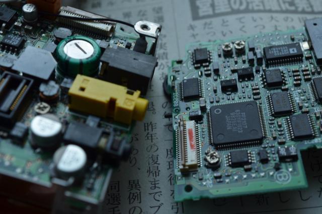
Even the most skilled engineers can make mistakes while designing printed circuit boards (PCBs). However, understanding where one could go wrong minimizes the engineering efforts, enhances productivity, and cuts down on the number of revisions. In 2022, this global PCB design software industry was estimated to be worth US$ 3.56 billion and is forecasted to expand at a CAGR of 12.3% during the period of 2023-2030. There are many mistakes one can make while trying to optimize a PCB software workflow, which one has to carefully avoid.
Missing DRCs
Errors such as shorts, clearance violations, and manufacturability infringements can occur when Design Rule Checks (DRC) are set aside. It is advisable not to run DRCs too late and always have intra-stage DRCs in the workflow to reduce expensive rework.
Suboptimal Component Placement
Signals may suffer from integrity degradation as well as robust routing from poor component layout. Related components should be clustered cleanly and spaced intelligently to minimize coupling and assist trace routing.
Inappropriate Trace Width & Spacing
Short circuits can be generated with inadequate spacing, and overheating can happen with signal traces that are too narrow. Set design rules for minimum spacing and thickness of the traces to ensure currents are within the limits and use the optimization tools in the PCB software.
Ground Planes and Power Distribution Are Under Consideration
Implementing a solid ground plane is necessary to contain noise and maintain stable signal performance. The quality of the power ground can cause electromagnetic interference (EMI) and power integrity problems. Careful planning of your power distribution and ground plane will enhance your PCB design performance.
Thermal Management Is Not Considered
Decreased performance is perhaps caused by component overheating. Address thermal challenges with respect to thermal vias, heat sinks, and sufficient separation from heat sources to improve reliability and minimize overheating.
Mismanaged Via Usage
Vias are either not used correctly, or they are used in excess, or inappropriately, which can damage the signal and increase manufacturing costs. Place vias according to the PCB design complexity and use the right types of vias, like blind vias, buried vias, and through-holes.
Signal Integrity Is Not Considered
Careless use of the signal can create signal reflection and crosstalk problems. For a better high-speed PCB design, be sure to simulate the circuit in your PCB software and check the signal's behavior so the right impedance is matched before the layout is done.
Ignoring Constraints around Manufacturing
Constructing designs without considering the manufacturer’s design constraints can cause issues in timelines and expensive redesigns. Always confirm constraints like drill dimensions, solder mask reliefs, and paneling for faultless fabrication.
Lack of Control on Library and Its Versions
Older component libraries with outdated versions can be problematic during the assembly of circuits. Control library updates and constrain the designs with appropriate versioning to retain design integrity and reduce mass production issues.
Design Documentation Issues: Missing Elements
Issues in design documentation, like missing or wrong Gerber files and drill files, can pose problems during fabrication processes. A thorough review of all PCB design files should be conducted before submission to greatly reduce production issues.
Final Thoughts
Following these best practices and eliminating these common PCB design pitfalls will allow professional and efficient PCB design of reliable and high-performance PCBs. Efficient use of PCB design software will lead to increased productivity and reduced expensive design faults.


